What CoWoS is
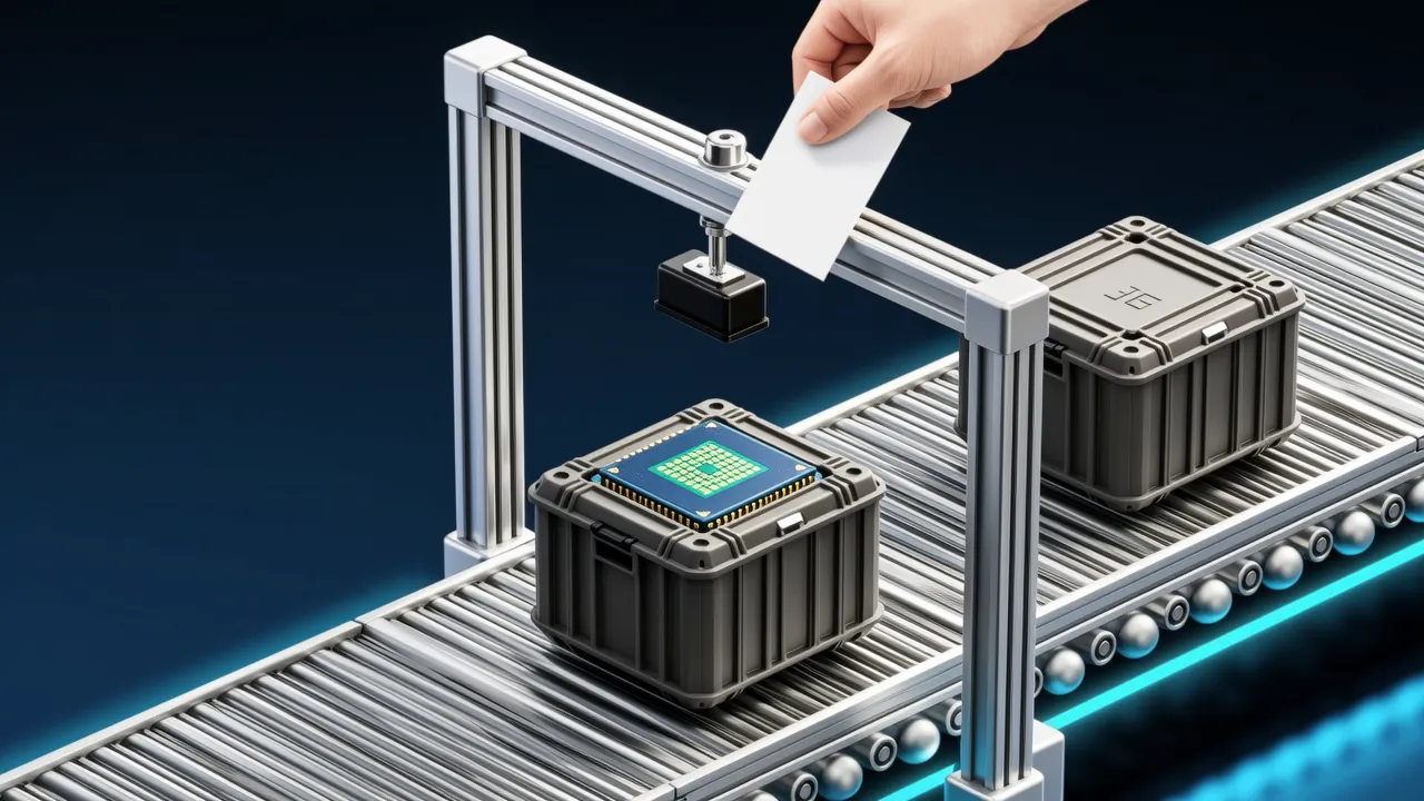
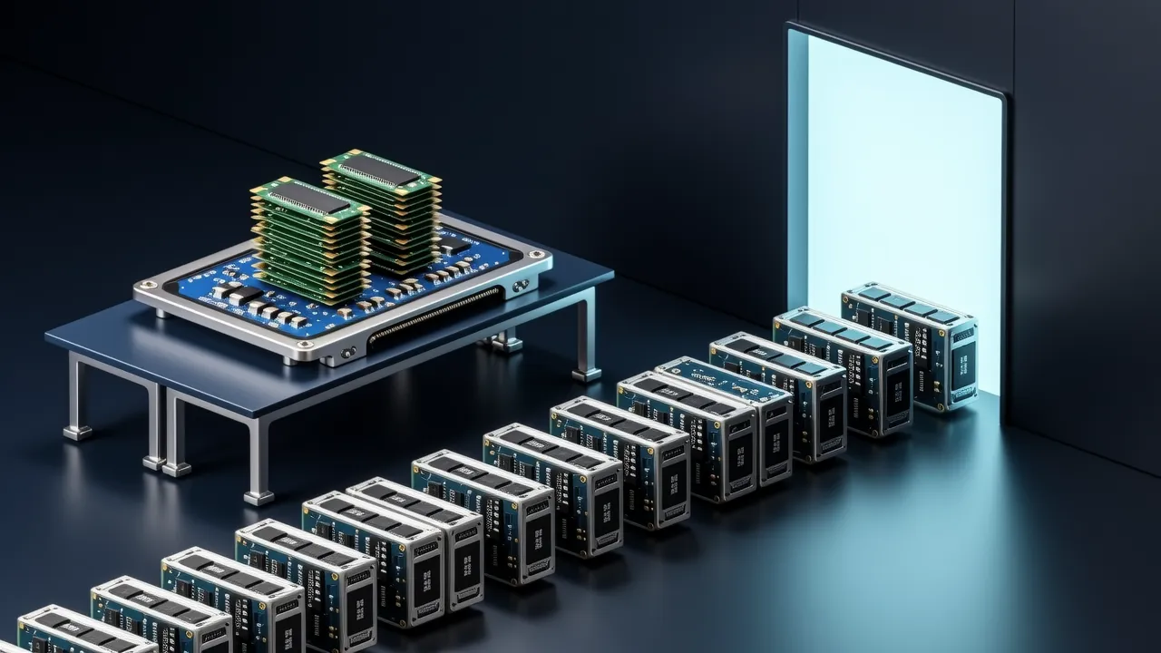
CoWoS stands for chip on wafer on substrate. It is TSMC's advanced packaging platform: logic dies and high-bandwidth memory (HBM) stacks are first mounted on a silicon interposer, and the interposer is then attached to an organic substrate.[1] Packaging comes after wafer fabrication and decides how many dies and how much memory can be wired together inside one package, so it shapes what a finished product can look like rather than simply housing it.
Why capacity is tight
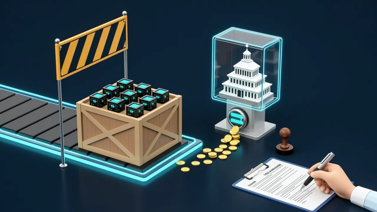
TSMC's CoWoS lines remain short of demand, and the platform's capacity is fully booked.[1] The pressure spreads to the wider supply chain: ASE Technology and other outsourced assembly firms are expanding their own advanced packaging capacity while CoWoS stays full.[1]
Where the expansion is going
At an investor conference, TSMC chairman and chief executive C.C. Wei said the company would keep investing in advanced packaging plants in Taiwan.[1] The build-out is concentrated in Tainan and Chiayi, where TSMC is converting mature-node fabs and building new packaging plants.[1][2] Because CoWoS is still in short supply, the company also plans to convert existing 8-inch wafer fabs in Taiwan into advanced packaging plants.[1]
How fast the numbers grow
Investment analysts cited by Central News Agency estimated that TSMC's CoWoS capacity would rise from about 70,000 wafers per month at the end of 2025 to 100,000 by the end of 2026 and 130,000 by the end of 2027.[1] TrendForce, citing institutional investors, gave a higher range: around 115,000 to 140,000 wafers per month by the end of 2026, and about 170,000 per month in 2027.[2] The two sets of figures do not match, which is usual for estimates made from outside a company, but both describe rapid growth over the same period.
Larger packages, SoIC and CoPoS
Wei said TSMC continues to offer the industry's largest reticle-size packaging, and that together with its SoIC platform the company is confident of giving customers the best options.[2] TSMC is also developing CoPoS, a chip-on-panel-on-substrate technology, whose pilot line completed major equipment installation in February 2026.[2] Market participants expect CoPoS to reach mass production in 2028 to 2029, with wider adoption in the following years.[2] Panels are larger than round wafers, which is the usual argument for panel-level packaging: a bigger working area means more dies can be processed together in one step.
Why it matters
For chip designers, CoWoS capacity sets a limit on how many high-end accelerators can be built in a given period, because the logic die and the HBM stacks are joined precisely at this packaging step. When TSMC's own lines are full, part of that work moves to assembly specialists such as ASE Technology, which are adding capacity of their own.[1] The expansion in Tainan and Chiayi therefore matters beyond TSMC: it is one of the places where the physical supply of AI hardware is decided.[1][2]
The longer-term answer TSMC is preparing is CoPoS, which shifts the carrier from a wafer to a panel and is not expected to reach mass production until 2028 to 2029.[2] Until then, the company's answer to tight capacity is more fabs converted and more plants built in Taiwan.[1]
Sources
- 1
- 2
Cite this page: TSMC CoWoS packaging stays sold out as AI demand outruns capacity. TellWorld, https://www.tellworld.net/news/cowos-supply-2026. Updated 2026-11-08