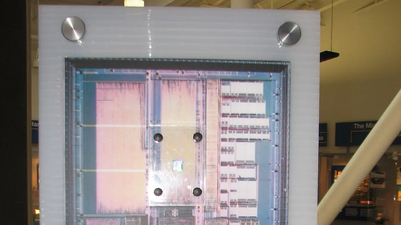

Why build a chip that imitates neurons
Most digital chips compute by shuttling data back and forth between a processor and memory, and they advance on a clock whether or not there is anything to do. Neuromorphic (brain-inspired) computing takes a different route. It represents information as spikes: a spiking neuron stays quiet until its input crosses a threshold, then emits a brief pulse that travels to whatever it is connected to. A silent neuron costs almost nothing, so the energy a chip draws tends to follow the activity of the network rather than the size of the hardware. The engineering difficulty is building such a network on a large scale out of silicon that can actually be manufactured.
What was published
On 8 August 2014, Science carried the paper "A million spiking-neuron integrated circuit with a scalable communication network and interface," in volume 345, issue 6197, pages 668 to 673 [1]. It has twenty authors, running from Paul A. Merolla and John V. Arthur to Dharmendra S. Modha [1]. The chip it describes was built at IBM and became known as TrueNorth.
The numbers on the chip
The circuit packs 5.4 billion transistors and 4,096 neurosynaptic cores, the repeated building blocks that hold and connect the neurons, tied together by a network on the chip itself [1]. Together those cores integrate 1 million programmable spiking neurons and 256 million configurable synapses, the junctions across which one neuron's pulse reaches the next [1]. The BBC reported that each neuron on the chip connects to 256 others [2], which matches the ratio between the reported synapse and neuron counts.
Energy use
As a demonstration of what such a network costs to run, the chip consumed 63 milliwatts while taking 400-pixel-by-240-pixel video at 30 frames per second as its input [1]. That is a small fraction of a watt, and it is the figure that made the design notable: a network with a million neurons was running on power in the range of small battery-powered electronics.
Scaling by tiling
The design was not meant to stop at one chip. Chips can be tiled in two dimensions through an interchip communication interface, which scales the architecture into a cortex-like sheet of arbitrary size [1]. The individual chip is therefore presented as a repeating unit rather than a fixed, finished machine.
How it was received
The BBC reported that the design was dubbed TrueNorth and described it as a supercomputer the size of a postage stamp [2]. The same report noted that the project amounted to more than 200 person-years of work [2], a figure that gives a sense of how much engineering sat behind a chip that fits in the hand.
What the paper left behind
The paper's contribution is a set of measured numbers rather than a promise. It put concrete counts on a single piece of silicon, 1 million neurons and 256 million synapses, gave a power measurement for a defined input stream, and sketched a route to larger systems by tiling chips in two dimensions [1]. That combination made the work a reference point: a claim about brain-scale hardware could now be stated in transistors, cores, neurons, synapses, milliwatts and a tiling scheme, and checked against a published device. The efficiency figure belongs to one particular input and network, so it is a measurement of that demonstration rather than a guarantee for every workload. What the paper established was that a spiking architecture could be built at this scale in ordinary silicon and connected into something larger.
Sources
- 1
- 2
Cite this page: IBM publishes the TrueNorth neuromorphic chip in Science. TellWorld, https://www.tellworld.net/news/ibm-truenorth-2014. Updated 2026-11-07